What is it about?
This work focusses on the metal-semiconductor contact on n-type c-Si wafers and explore the possibility of using magnesium (Mg) to form electron–selective contacts instead of using the conventional Au-Sb films which requires high temperature annealing between 350 and 500 °C. Aluminium (Al) capping layer was added over the magnesium contacts to prevent oxidation of magnesium. Various electrical measurements were performed over thermally evaporated Mg/Al contacts to investigate the conduction properties on both p-type and n-type silicon, where a Schottky behaviour was observed for the p doped silicon, but an ohmic behaviour (V ∝ I) for the n-type doped c-Si samples. The results were further optimised after investigating various thicknesses of the Mg interlayer, with 10 nm of Mg interlayer found to have the least resistance. The resistivity of the optimised structure (n-Si/Mg-10 nm/Al) was calculated, and measurements according to the Transmission Line Method (TLM) showed a contact resistivity of 462 mΩ cm2 ± 20 mΩ cm2. Further investigations were also conducted on the effect of high temperature annealing of the magnesium contact, which showed an increase in resistance with increase in annealing temperature, with the lowest resistance obtained without annealing. Additional investigations focussed on the morphological analysis of the deposited magnesium and its impact on the electrical characteristics.
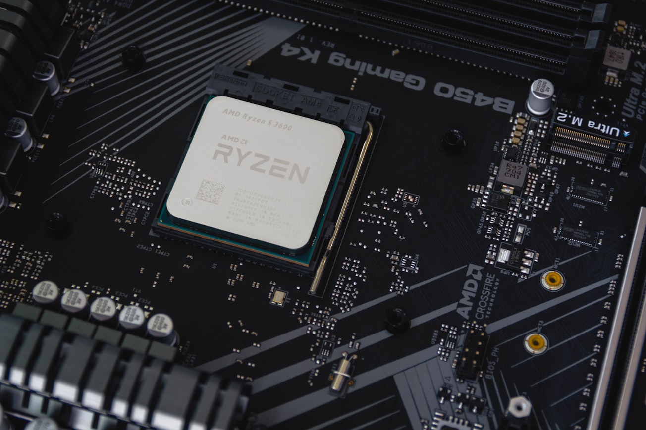
Featured Image

Photo by Christian Wiediger on Unsplash
Why is it important?
This work highlights the advantages of using Mg (capped with Al) as an ohmic contact with n-type c-Si wafers, eliminating the need for energy intensive high-temperature annealing in inert atmospheres for hours, use of Au -Sb alloy. Hence, using Al-Mg with n-type c-Si, the formation of ohmic contact could be accomplished in a single-step process at room temperature, thereby offering a possibility of reductions in semiconductor device manufacturing costs, as well as energy requirements and carbon footprint.
Perspectives
The authors learnt a great deal of misconception of explaining the ohmic contact, saying work function of semiconductor rather than bringing the concept of electron affinity, by various workers.
Professor Shashi Paul
De Montfort University
Read the Original
This page is a summary of: Single step ohmic contact for heavily doped n-type silicon, Applied Surface Science, November 2019, Elsevier,
DOI: 10.1016/j.apsusc.2019.144686.
You can read the full text:
Resources
Contributors
The following have contributed to this page


