What is it about?
In this paper, a unique technical approach is presented to accurately analyze and optimize the address bus of an onboard DDR4 memory module by taking power plane induced noise and thermal effect simultaneously in the analysis.
Featured Image
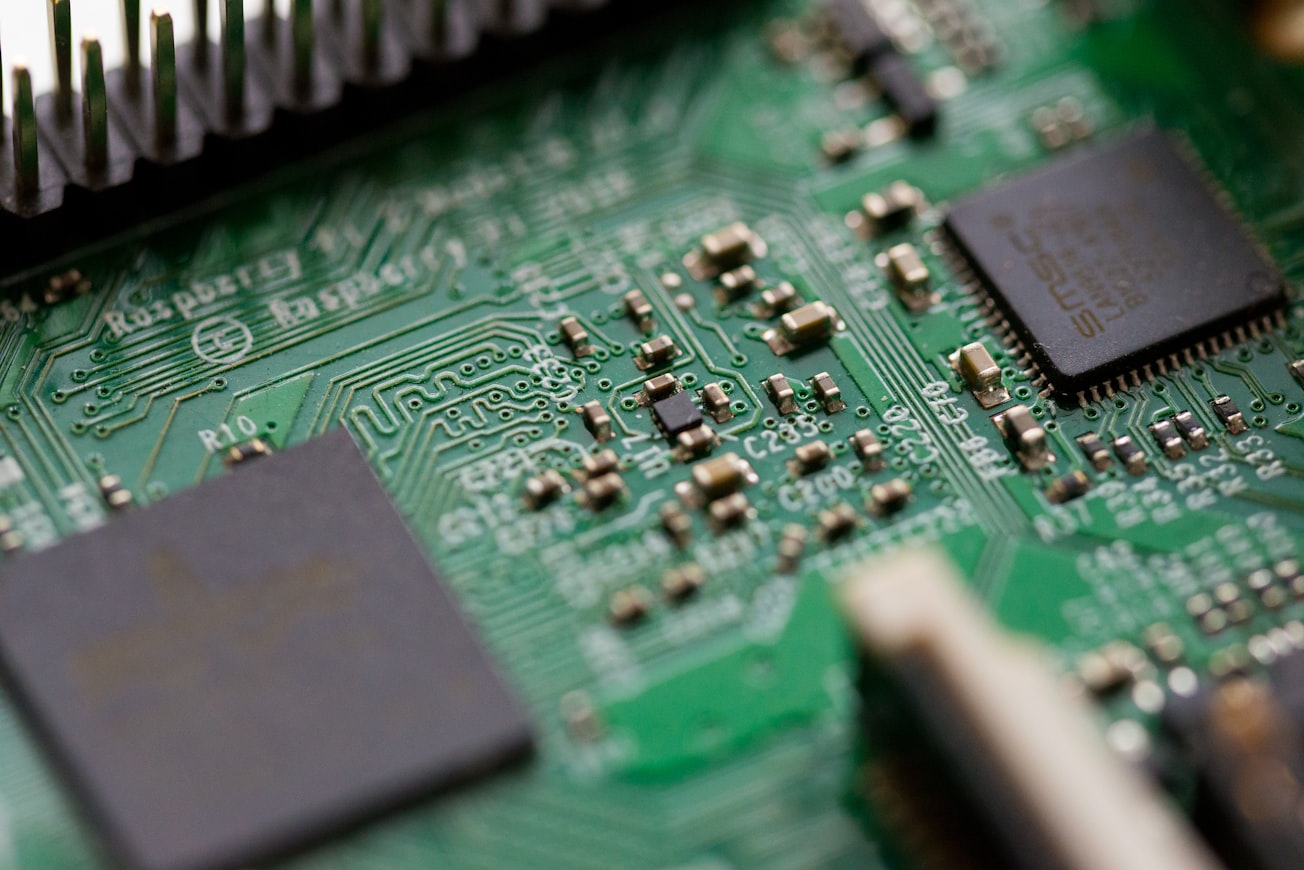
Photo by Chris Ried on Unsplash
Why is it important?
In high-speed digital (HSD) board design, it’s crucial to accurately characterize power delivery network (PDN) and address bus by considering both power supply induced jitter and overall thermal effect in simulation to make sure that digitally transmitted 1s and 0s look like same at the receiver. Due to simulation tools limitations, most of the customers perform power integrity (PI), thermal analysis and signal integrity (SI) analysis separately that doesn’t guarantee accurate and reliable data signal performance. Signal integrity and Power Integrity analysis of DDR4 (Double Data Rate fourth-generation) address bus are necessary for the data reliability and robustness. DDR4 has single ended signals at 3.2 Gbps data rates. With such high data rates, the time between various operations decrease and it increases the magnitude of signal integrity effects. In DDR4, the twomain category of buses involved are the data and address, control and command buses.
Perspectives
In DDR4 memory module, the address bus is a multi point unidirectional connection from a controller IC to the memory modules so it's really important to eliminate all SI-PI related issues from design before fabrication.
RF | Microwave | Antenna | Signal Integrity Engineer Anil Pandey
Keysight Technologies
Read the Original
This page is a summary of: Signal and power integrity analysis of DDR4 address bus of onboard memory module, December 2018, Institute of Electrical & Electronics Engineers (IEEE),
DOI: 10.1109/edaps.2018.8680896.
You can read the full text:
Resources
Contributors
The following have contributed to this page


